
Key Benefits
- Rapid evaluation and feasibility of potential interconnect pathways in a single-canvas view of die/package/PCB substrates and cross-substrate interconnect
- Efficient evaluation and tradeoff providing better prediction of cost and performance using well-qualified design definitions
- A smooth predictable path to optimized in-substrate and cross-substrate routing
- Optimized signal performance while minimizing overall design time by avoiding late-cycle design changes
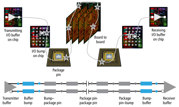
ALMOST EVERY CHIP MUST BE PACKAGED AND THEN DESIGNED INTO A SYSTEM OR SUBSYSTEM THAT IS USUALLY REPRESENTED AS A PCB. SIGNALS, ESPECIALLY IMPORTANT SIGNALS THAT MUST PERFORM TO A PROTOCOL STANDARD SUCH AS DDRX MEMORY OR HIGH-SPEED SERIAL SUCH AS PCI EXPRESS® (PCIE®), MUST TRANSITION ACROSS THE THREE OR MORE VERY DIFFERENT SUBSTRATES AND REACH THEIR TARGET WITHIN SPECIFICATION.
AGAINST THEM ARE THE MATERIALS AND PROPERTIES OF THE SUBSTRATES, AND OF COURSE THE INTERCONNECT PATHWAYS BETWEEN THE SUBSTRATES AND THEIR TRANSITION POINTS (DIE BUMPS, PACKAGE BGA BALLS, AND PCB BREAKOUT PATTERN). THIS SYSTEM-LEVEL INTERCONNECT IS SUMMARIZED IN FIGURE 1.
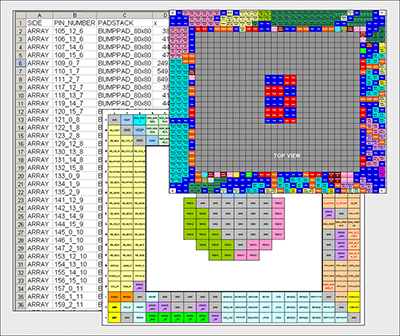
In every semiconductor company or systems company that is designing an IC is a person or persons responsible for defining the IC bump and package ball arrays or patterns and signal, power, and ground assignments. It’s very common for this to be done using spreadsheets, such as the one in Figure 2.
The problem with spreadsheets is that they are manual, error prone, use static data from the design tools, and cannot effectively or efficiently communicate interconnect routing instruction or constraints to the upstream and downstream implementation tools. Yes, spreadsheets can be effective for pin and net assignments, but what about:
- Signal/power/ground (SPG) ratios and patterning to ensure quality return paths and power delivery
- Route pathways for escape sequencing, layer assignments, and feasibility
- Bottom-up or PCB-driven assignment, or pin compatibility with previous-generation designs
- Diff pair management and propagation across the substrates
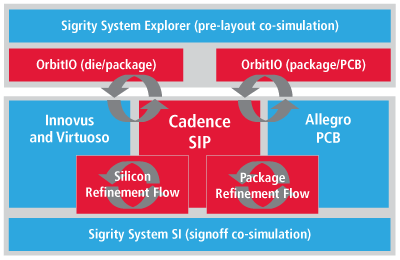
Using spreadsheets can now be a thing of the past as multi-substrate interconnect exploration, definition, and design can now be done in Cadence’s integrated solution (Figure 3): Cadence® OrbitIO™ Interconnect Designer and Allegro Package Designer SiP Layout Option.
Design Flow
The OrbitIO Interconnect Designer transforms the cross-substrate interconnect architecting, assessment, implementation, and optimization process by unifying IC, package, and PCB data in a single environment where signal-to-bump/ball-assignment and connectivity/routing-pathway scenarios are easily derived and evaluated in the context of the complete system prior to implementation. Full system visualization and a unified data model enable rapid exploration and propagation of changes to adjacent substrates, providing instantaneous feedback on their system-wide impact. OrbitIO Interconnect Designer helps the engineer/architect achieve the right balance of cross-substrate interconnect integration for optimal performance, cost, and manufacturability prior to implementation—resulting in fewer iterations and shorter cycle times.
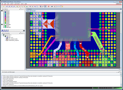
Within a single graphical, lightweight, and easy-to-use environment (Figure 4), the following can be rapidly explored, defined, and communicated:
- Geometrical definition of bump and ball pad patterns
- Pin-based floorplannin
- Allocations of pins or regions for use by specific signal types or interfaces
- Power delivery and return path planning
- Netlist definition and management
- Propagation and mapping of nets between fabrics
- Route pathway exploration, definition, and optimization
- Connection sequencing and assignment
- Evaluate route feasibility
- Communication of results and intent to the fabric implementation teams
OrbitIO Interconnect Designer does not restrict you to a single methodology, instead it has been designed to enable the most common interconnect pathway methodologies commonly used today:
- IC/PC-driven package BGA ball map design and optimization, including PCB schematic symbol generation (DE-HDL support)
- IC-driven BGA ball map design and optimization
- Cross-substrate IC bump array and package ball definition and optimization with route pathway design including PCB
- Early package start-from-nothing BGA ball map creation
- Package BGA-driven IC bump array design and optimization
- Package BGA ball map-based design and optimization targeting multiple PCBs (variants-based design)
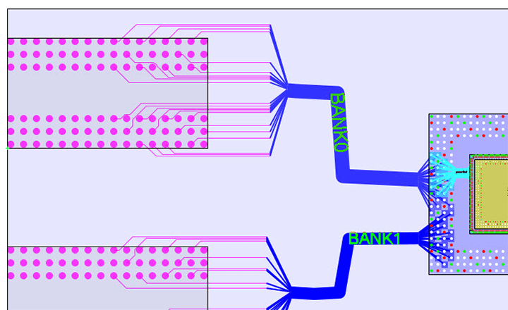
Figure 5 shows an example of the first methodology. Here a pre-placed PCB with two fixed DDR3 memory devices is driving the assignment and route pathway plans onto the package BGA and up to the IC bump array.
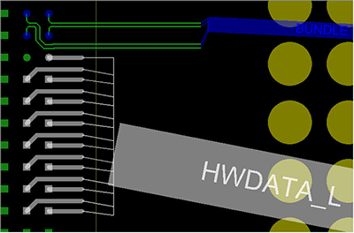
Once the critical signals and buses have been explored, defined, and evaluated, the resultant pathways can be handed off to the respective substrate implementation designers and design tools for detailed manufacturing rules-driven implementation (Figure 6).
With the OrbitIO Interconnect Designer and SiP Layout Option solution, you now have an environment for the rapid evaluation and feasibility of potential interconnect pathways in a single-canvas view of die/package/PCB substrates and cross-substrate interconnect. This solution enables efficient evaluation and tradeoff providing better prediction of cost and performance using well-qualified design definitions. Direct integration with the IC implementation tools (Innovus™ and Virtuoso® solutions) as well as the IC package implementation tool (SiP Layout Option) provides a smooth predictable path to optimized in-substrate and cross-substrate routing, leading to optimized signal performance while minimizing overall design time by avoiding late-cycle design changes.
以下内容为机器自动翻译,可能存在翻译不准确的情况
统一IC、软件包和PCB数据,以便轻松派生和评估信噪-碰撞/球分配和连接/路由路径场景
主要好处
- 在模具/包装/PCB衬底和跨衬底互连的单画布视图中快速评估和可行性潜在的互连路径
- 高效的评估和权衡,使用合格的设计定义更好地预测成本和性能
- 优化基板内和跨基板路由的平稳可预测的路径
- 优化信号性能,同时通过避免后期设计更改来最大限度地减少整体设计时间
几乎每个芯片都必须打包,然后设计成通常表示为PCB的系统或子系统。信号,特别是必须按照DDRX内存等协议标准或PCI EXPRESS®(PCIE®)等高速串行执行的重要信号,必须跨越三个或更多非常不同的基板过渡,并在规格范围内达到目标。
衬底的材料和性能是衬底的材料和性能,当然还有衬底与其过渡点之间的互连通路(死亡碰撞、包装BGA球和PCB突破模式)。图1总结了这种系统级互连。
在设计集成电路的每家半导体公司或系统公司中,都有一个或多个负责定义集成电路碰撞和封装球阵列或模式以及信号、功率和地面分配的人。使用电子表格(如图2中的电子表格)来做到这一点是非常常见的。
电子表格的问题在于,它们是手动的,容易出错,使用设计工具中的静态数据,无法有效或高效地将互连路由指令或约束传达到上游和下游实现工具。是的,电子表格对引脚和网络分配可能有效,但呢:
- 信号/功率/地面(SPG)比率和模式,以确保高质量的返回路径和电力输送
- 逃逸测序、图层分配和可行性的路由路径
- 自下而上或PCB驱动的分配,或与上一代设计的引脚兼容性
- 不同的对管理和跨基板的传播
使用电子表格现在可以成为过去,因为多基板互连探索、定义和设计现在可以在Cadence的集成解决方案(图3):Cadence® OrbitIOTM互连设计器和Allegro Package Designer SiP布局选项中完成。
设计流程
OrbitIO互连设计器通过在单个环境中统一IC、包和PCB数据来转换跨基板互连架构、评估、实现和优化过程,在实现前,信号到碰撞/球分配和连接/路由路径场景可以在完整系统中轻松派生和评估。完整的系统可视化和统一的数据模型可以快速探索和传播对相邻基板的变化,就其全系统的影响提供即时反馈。OrbitIO互连设计器帮助工程师/架构师在实现跨基板互连集成的正确平衡,以实现最佳性能、成本和可制造性,从而减少迭代和缩短周期时间。
在单一的图形化、轻量级和易于使用的环境中(图4),可以快速探索、定义和沟通以下内容:
- 凸起和球垫图案的几何定义
- 针基地板
- 用于特定信号类型或接口的引脚或区域的分配
- 电力输送和回电路径规划
- Netlist定义和管理
- 织物之间网的繁殖和映射
- 路线路径探索、定义和优化
- 连接顺序和分配
- 评估路线可行性
- 向结构实施团队传达结果和意图
OrbitIO互连设计器不将您限制在单一方法上,而是旨在启用当今常用的最常见的互连路径方法:
- IC/PC驱动的软件包BGA球形图设计和优化,包括PCB原理图符号的生成(支持DE-HDL)
- IC驱动的BGA球图设计和优化
- 跨基IC凸起阵列和封装球的定义和优化,包括PCB在内的路径设计
- 早期软件包从头开始BGA球图创建
- 软件包BGA驱动的IC凸起阵列设计和优化
- 基于BGA球图的包装设计和优化,针对多个多氯联苯(基于变体的设计)
图5显示了第一种方法的示例。在这里,带有两个固定DDR3内存设备的预置PCB正在将分配和路由路径计划驱动到软件包BGA和IC凸起阵列。
一旦对关键信号和总线进行了探索、定义和评估,由此产生的路径可以移交给各自的基板实现设计器和设计工具,以进行详细的制造规则驱动的实现(图6)。
使用OrbitIO互连设计器和SiP布局选项解决方案,您现在有一个环境,以便在模具/包装/PCB基板和跨基板互连的单画布视图中快速评估和可行性潜在的互连路径。该解决方案允许使用合格的设计定义进行高效的评估和权衡,从而更好地预测成本和性能。与IC实现工具(InnovusTM和Virtuoso®解决方案)以及IC包实现工具(SiP布局选项)直接集成,为优化基板内和跨基板路由提供了一条平稳可预测的路径,从而优化信号性能,同时通过避免后期设计更改最大限度地减少整体设计时间。
