
Key Benefits
- Ensure both electrical and thermal integrity of PCB
- Reduce cost while maintaining performance by optimizing decoupling capacitorsEnsure both electrical and thermal integrity of PCB
- Quickly and accurately analyze large PCBs for both AC and DC power integrity
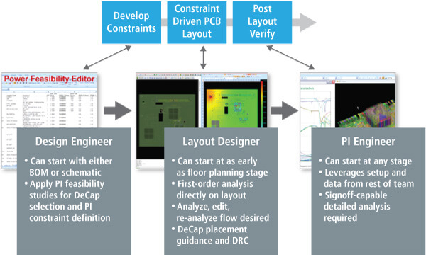
The team-based approach to power integrity starts early in the design process when selecting decoupling capacitors and adding them to the schematic. The Cadence®Allegro® Sigrity™ PI analysis enables passing this design intent to layout designers through constraints and much more. You are further enabled with DC analysis technology and then PI experts can step in and validate the finalized design for AC and DC performance, ensuring that the power delivery network (PDN) is working to spec and fully optimized.
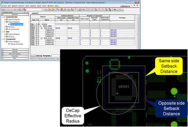
With low power becoming a high priority for electronic designs, power integrity can no longer be an afterthought. A constraint-driven power integrity flow keeps PDN design as a forethought throughout the design process. The Cadence Sigrity team has expanded on the proven constraint-driven flow for signal integrity and recently added constraint sets that are specific for power integrity. Allegro Sigrity PI technology supports the full design flow by enabling the capture of PI Csets early and guiding PCB designers to follow the constraints associated with decoupling capacitor selection and placement. But the PCB designer’s job doesn’t stop there. When using Allegro Sigrity PI, PCB designers can run IR drop analysis and find locations where the PDN cannot deliver sufficient voltage. So not only are they able to properly decouple a design, they are empowered to address first-order DC concerns.
When the design is complete and power integrity signoff is required, PI experts can use the Allegro Sigrity PI solution to run full-featured AC and thermal-aware DC analysis tools as well as decoupling capacitor optimization. With access to the Allegro PCB Editor, the experts can easily communicate to PCB designers what needs to be accomplished to both optimize and signoff on the power delivery network design.
With a power delivery network validated with the Allegro Sigrity PI solution, you can build your design with confidence knowing that efficient, sufficient, and stable power will be delivered to the components on your design and that product creation time will be minimized.
以下内容为机器自动翻译,可能存在翻译不准确的情况
主要好处
- 确保PCB的电气和热完整性
- 通过优化解耦电容器来降低成本,同时保持性能,确保PCB的电气和热完整性
- 快速准确地分析大型多氯联苯,以实现交流和直流电源完整性
在选择解耦电容器并将其添加到原理图中时,基于团队的电源完整性方法始于设计过程的早期。Cadence® Allegro® SigrityTM PI分析允许通过约束等将这种设计意图传递给布局设计师。您进一步启用了直流分析技术,然后PI专家可以介入并验证交流和直流性能的最终设计,确保供电网络(PDN)正在规范和完全优化。
随着低功耗成为电子设计的重中之重,功耗完整性不再是事后的想法。约束驱动的功率完整性流使PDN设计在整个设计过程中成为一种先见之宝。Cadence Sigrity团队扩展了经过验证的信号完整性约束驱动流,最近添加了特定于电源完整性的约束集。Allegro Sigrity PI技术支持整个设计流程,使PI Cset能够及早捕获,并指导PCB设计师遵循与解耦电容器选择和放置相关的限制。但PCB设计师的工作不止于此。使用Allegro Sigrity PI时,PCB设计人员可以运行红外下降分析,并找到PDN无法提供足够电压的位置。因此,他们不仅能够正确地解耦设计,还有权解决一阶DC问题。
当设计完成并需要电源完整性签核时,PI专家可以使用Allegro Sigrity PI解决方案运行功能齐全的交流和热感知直流分析工具以及解耦电容器优化。通过访问Allegro PCB编辑器,专家可以轻松地与PCB设计师沟通优化和签收电力输送网络设计需要完成的工作。
通过使用Allegro Sigrity PI解决方案验证的电力输送网络,您可以自信地构建您的设计,因为您知道高效、充足和稳定的电力将交付到您设计的组件,并且产品创建时间将最小化。


